Amateur Extra Question E6C11
E6C: Digital ICs: families of digital ICs; gates; programmable logic devices
In Figure E6-3, which is the schematic symbol for the NOT operation (inversion)?
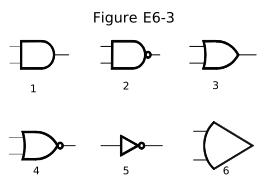
- 2
- 4
- 5 (correct answer)
- 6
Correct answer: C, 5
Explanation
An inverter (NOT gate) has one input and one output. Its output is always the opposite of its input. Its symbol is a triangle pointing toward the output with a small circle, the inversion bubble, at the tip. In Figure E6-3, symbol 5 is the only one with a single input and a triangle body, and it has the bubble on its output. The bubble always means inversion, but only the triangle-plus-bubble shape is the NOT operation by itself.
Why the other answers are wrong
- A, 2: Symbol 2 has the flat back and D-shaped body of an AND gate plus an output bubble, so it is a two-input NAND gate, not a one-input inverter.
- B, 4: Symbol 4 has the curved input side and pointed tip of an OR gate plus an output bubble, so it is a two-input NOR gate, not a one-input inverter.
- D, 6: Symbol 6 has the curved input side of the OR family and two inputs, and it has no inversion bubble, so it cannot be a simple inverter.